Data Flow Modelling in Verilog
Web Half adder is a combinational arithmetic circuit that adds two numbers and produces a sum bit S and carry bit C as the output. Web Data flow modeling.

Gate level modeling enables us to describe the circuit using these gate primitives.
. They are Dataflow Gate-level modeling and behavioral modeling. Dataflow modeling uses expressions instead of. Theres no need for data- type declaration in this modeling.
Gate level modelling is compared with Data flow modelling with the help of few exampleslin. Web Verilog provides us with gate primitives which help us create a circuit by connecting basic logic gates. While the gate-level and dataflow modeling are used for combinatorial circuits behavioral modeling is used for both sequential and combinatorial circuits.
It is a setup to test our Verilog code. We start by writing include which is a keyword to include a file. Web Dataflow Modeling.
This approach allows the designer to focus on optimizing the circuit in terms of the flow of data. Web Learn to design Combinational circuits using data Flow modelling. Web Verilog full adder in dataflow gate level modelling style.
First of all we declare the module. Then we use assignment statements in data flow modeling. Web Verilog Language is a very famous and widely used programming language to design digital IC In this verilog tutorial level of abstraction has been covered.
Endmodule Just like the and operation the logical operator performs a binary multiplication of the inputs. There are three types of modeling for Verilog. Assign couta.
The design is compared with hierarchical design. Dataflow modeling in Verilog allows a digital system to be designed in terms of its function. Dataflow modeling has become a popular design approach as logic synthesis tools became sophisticated.
Given below is the logic diagram of an SR Flip Flop. The test bench is the file through which we give inputs and observe the outputs. It includes the Verilog file for the design.
The two basic logic gates are AND and OR gates in which the name suggested. Web Verilog code for AND gate using data-flow modeling. So if i want to describe a 2 to 4 decoder in dataflow modeling i would be like this.
SR flip flop logic circuit. We would again start by declaring the module. Assign Y A.
If neither input is high the output is low 0. An OR gate is a logic gate that performs a logical OR operation. Web However in complex design designing in gate-level modeling is a challenging and highly complex task and thats where data-flow modeling provides a powerful way to implement a design.
From the above circuit it is clear we need to interconnect four NAND gates. Web Dataflow modeling makes use of the functions that define the working of the circuit instead of its gate structure. Verilog allows a circuit to be designed in terms of the data flow between registers and how a design processes data rather than the instantiation of individual.
Verilog code for 21 MUX using data flow modeling. Web Data flow modelling in Verilog and Implementation of BCD Adder in Xilinx ISE. To start with this first you need to declare the module.
Web To get familiar with the dataflow and behavioral modeling of combinational circuits in Verilog HDL Background Dataflow Modeling Dataflow modeling provides the means of describing combinational circuits by their function rather than by their gate structure. Full Adder in Dataflow model. Remember that a module is a basic building block in Verilog.
A logical OR operation has a high 1 output when one or both of the gates inputs are high 1. Module AND_2_data_flow output Y input A B. Web Testbench in Verilog of a half-subtractor.
Dataflow modeling uses a number of operators that act on operands to produce the. Web in this video 4-bit Adder has been designed and simulated using Data Flow Modelling. Web But before starting to code we need proper knowledge of basic logic gates in Verilog.
The following figure shows a basic NAND gate Gate Level Modeling Data Flow Modeling Behavioural Modeling RTL Simulation and Truth Table of NAND. Handling multi-bit data Concatenation to group data. Just like an AND gate an OR gate can have any number of input probes but only one output probe.
The first line is. Web Verilog Code for Full Subtractor using Dataflow Modeling. Module fulladder input a input b input cin output s output cout.
To declare the module we have a keyword module then we write the identifier or the name of the module in this way. The dataflow level shows the nature of the flow of data in continuous assignment statements. Dataflow modeling utilizes Boolean equations and uses a number of operators that can acton inputs to produce outputs operators like -.

Veriloghdl Basic Data Flow Modelling Youtube
What Is The Difference Between Data Flow And Behavioral Modelling In Verilog Hdl Ee Vibes
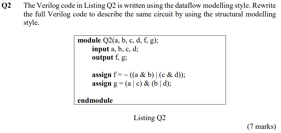
Solved The Verilog Code In Listing Q2 Is Written Using The Chegg Com

Lecture 4 Dataflow And Behavioral Modeling I Youtube

0 Response to "Data Flow Modelling in Verilog"
Post a Comment